
Good Things Come in Small Packages
 To keep up with the ever increasing demands of consumers’ expectations for increased computing power and mobility, the semiconductor industry strives to improve the performance and yield of new devices. By continuing to invest heavily in research and development efforts, chip-makers aim to design even smaller transistors and, thus, keep Moore’s Law alive (i.e., the number of transistors in a dense integrated circuit has doubled approximately every two years). In order to harness these advances and apply them in commercial products, the industry must develop the interface between the semiconductor chip and circuit board to maintain reliable communication while still minimizing the footprint of the device.
Traditionally, integrated circuit packages would consist of a leadframe with an island to which the chip is attached surrounded by leads with wirebonds connecting to the chip or a flip chip package with the chip attached with small solder balls to one side of a circuit board. In this case, the circuit board would have a number of wiring layers and another set of solder balls on the other side. These types of packages can take up a lot of real estate on a motherboard or can be overly thick. Thickness is obviously undesirable for use in mobile devices which are trending thinner and thinner. For example, the latest versions of the Apple and Samsung smartphones are 6.9mm and 6.8mm, respectively, and are a constant advertising point in the current mobile landscape.
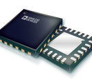
To enable mobile devices to include more features and higher processing power most now use a stacked package on package (PoP) solution with the main system memory piggybacking on top of the processor. The PoP can reduce communication latency and improve bandwidth. Smaller communication chips that provide the expected communication options, such as LTE, Bluetooth, and WiFi, often utilize a package with the absolute minimum area possible. Appropriately named chip-scale packages (CSP), these packages apply solder balls, which are used to connect the IC to a circuit board, at the surface of the device.
Beyond the processors and communication chips that need smaller packages, the myriad of the smartphones’ and wearable devices’ sensors also need to find space inside the device. As we are seeing with the new wave of wearables, adding sensors drives further development in size/efficiency. More and more devices and products need to become interconnected as the Internet of Things continues to develop. Other factors that make packaging improvements important include the need for devices to be more resistant to shock, temperatures, and humidity as mobile products accompany us in all aspects of our day to day lives—e.g., our daily commutes, exercise, entertainment, work, and even sleep.
Advanced packaging solutions have also provided an avenue for improving processing devices by directly stacking chips on top of each other in a three-dimensional chip. These chips connect from one surface of the semiconductor chip to the other with what is known as a ‘through-silicon via” or TSV. Reliability and manufacturing concerns related to heat dissipation and costs have made it difficult for companies to develop commercial products thus far. One of the first examples of commercial use is a joint venture between Intel and Micron. The partnership has been able to produce stacks of memory chips using TSV technology for use in graphics processing products in what they call a Hybrid Memory Cube. We will ikely see more smartphone cameras use chip stacking and TSVs, as some flagship mobile devices currently use a camera module with the image processing and control chip stacked directly on the sensor.
As consumers expect more and more features in smaller products, not only are the performances of semiconductor transistors critical but also the package in which they are contained. If the reliability and cost issues surrounding true 3D integration of stacking multiple dies can be solved, for example, it will likely open up new opportunities for increased memory and processing capabilities in devices from smartphones to super-computing systems.